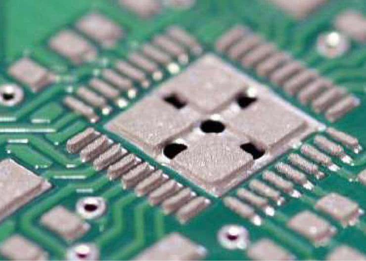
The proportion of components in SMD housings on PCBs of many new designs exceeds 90…95%. Smaller ratios generally apply to power conversion devices that contain components such as large inductances or high-current connectors. All other applications, for a variety of reasons, are moving almost entirely to surface mount. At the high-volume production stage, this has many advantages, but for prototyping and small batch manufacturing, it involves many difficulties. In this article we will explain how to cope with them, using professional equipment from the RENEX range..
Electronics design is becoming increasingly difficult. In the latest designs, it is becoming tricky to find compromises for many opposing technical issues. But it doesn’t stop there – for a project to have a chance of implementation, it must also meet industry standards, fit within budget assumptions, take into account component availability and ensure short lead times. Meeting all of these assumptions requires the use of modern solutions at every stage of the project.
Miniaturization
The most important reason for changes in the way new circuits are designed and prototyping techniques is the miniaturization of electronic component housings. The use of increasingly smaller housings is justified for several reasons:
- the final device is smaller and therefore also cheaper, but it also wins in terms of innovation, user comfort and functionality,
- modern components are mostly available only in miniature housings,
- problems with semiconductor availability have led to greater availability of chips with a narrower range of applications, i.e., those in miniature housings, among others..
Miniaturization in electronics means that even if only one piece of a prototype circuit is needed, it cannot be assembled by hand and fabrication requires a normal manufacturing process. This has a strong impact on electronics manufacturers, as given such an eventuality, they need to partner with a suitable co-operator or procure the right tools and equipment. Given that miniaturization in electronics is a progressive phenomenon, it is important to prepare for this trend in order not to fall out of business.
Soldering station as mandatory equipment
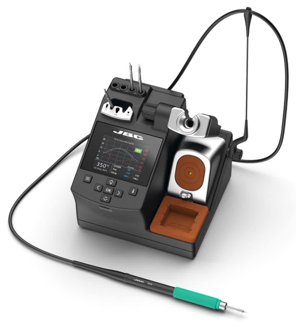
The vast majority of assembly work, including for miniature components the size of SMD0603 or even SMD0402, can be done with a soldering station. However, it must be a station developed specifically for such precise tasks, no universal devices will work well in such an application. An excellent choice is the JBC digital soldering station type JBC–CDE-2BQA (photo 1) equipped with the Soldering Assistant function.
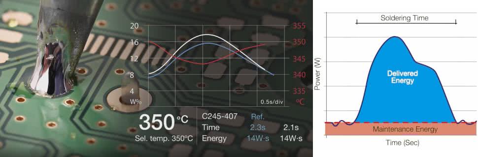
It is an innovative system that detects the various stages of the soldering process and automatically adjusts the parameters of the soldering iron. The operation of the system is illustrated in Figure 1, the optimal temperature characteristics guarantee the best soldering quality and increase the speed of work. The course of the soldering process and all settings are illustrated on a color graphic display (Figure 2).
It is worth noting that the operation of this system is only possible with the proper design of the heating module, in which the heater must be extremely strongly thermally coupled to a precision tip and temperature sensor to achieve ultra-low thermal inertia. This feature simultaneously enables frequent activation of sleep and hibernation modes, which help extend the life of the tip. Even when the temperature of the tip is lowered during a short period of inactivity, the working temperature is reached again in less than 2 seconds, which does not slow down the work at all.
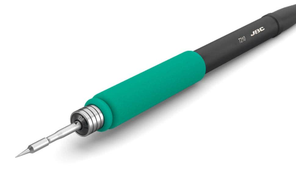
The station is equipped with a small T245 type iron measuring 145×20×20 mm with an exceptionally low weight of 0.07 kg. This allows for free and precise operation of this tool. If necessary, the station can be equipped with a precision T210-type iron measuring 123×14×14 mm and weighing even less than 0.06 kg (Photo 2). A rich assortment of tips will make many difficult tasks possible (Figure 3).


Pick and place for prototypes
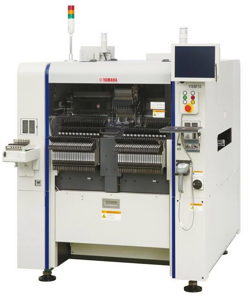
The use of components smaller than SMD0603 or circuits in multi-lead BGA or WCSP enclosures requires a normal manufacturing process. The main step in this process is automatic component placement. This is done using machines called pick and place for short, in which components are placed on special belts and then automatically distributed directly on the surface of the printed circuit. These are among the most complex parts of the assembly line, capable of operating at very high speeds. YAMAHA YSM10 (Photo 3) is a popular device of this type.
Application of solder paste
Solder paste is a composition of chemical materials that is a mixture of flux and finely powdered metals (solder), such as tin, lead, silver or copper, used in surface mount soldering (SMT – Surface Mounting Technology). This substance is applied to the pads of the components on the PCB even before the components are placed on it in the pick and place machine (Photo 4). The properties of the solder paste allow it to hold the components in the right places, and eventually, when heated, it becomes a solder joint that electrically and mechanically connects the components to the board.
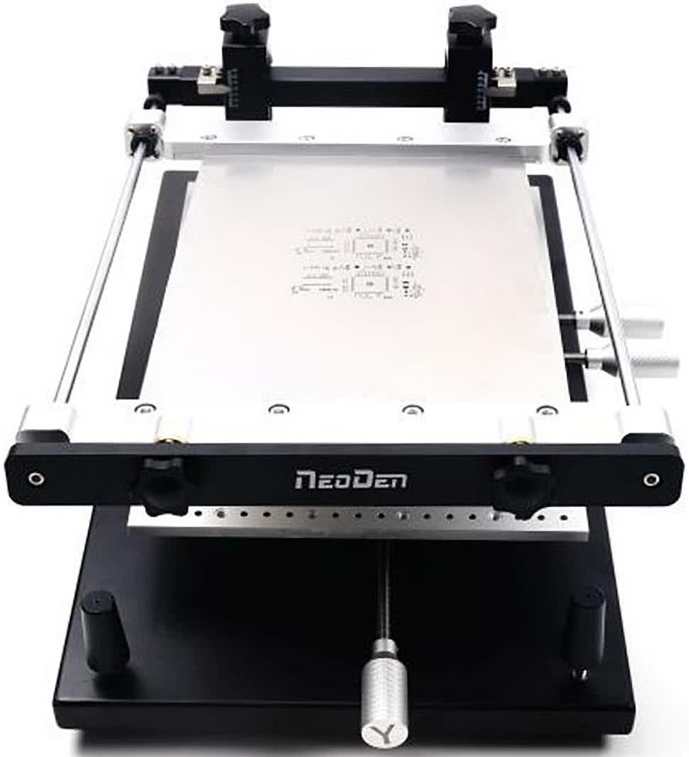
A device known as a Solder Paste Printing Machine is used to apply the paste. In the first phase, a board and a special metal template, made for each PCB design, are placed in the printer, containing holes in the areas to be distributed the paste (Photo 5). The templates are most often made from a sheet of stainless steel with laser-cut holes. Mutually precise and stable placement of both the board and the template is very important. When this happens, the machine spreads the paste over the surface of the stencil – thanks to the holes, the substance is placed only in the intended places on the board. An important issue is to control the amount of spread paste. The application of too much of it can cause spillage of solder joints leading to short circuits, while the application of too little can contribute to an incorrect solder joint.
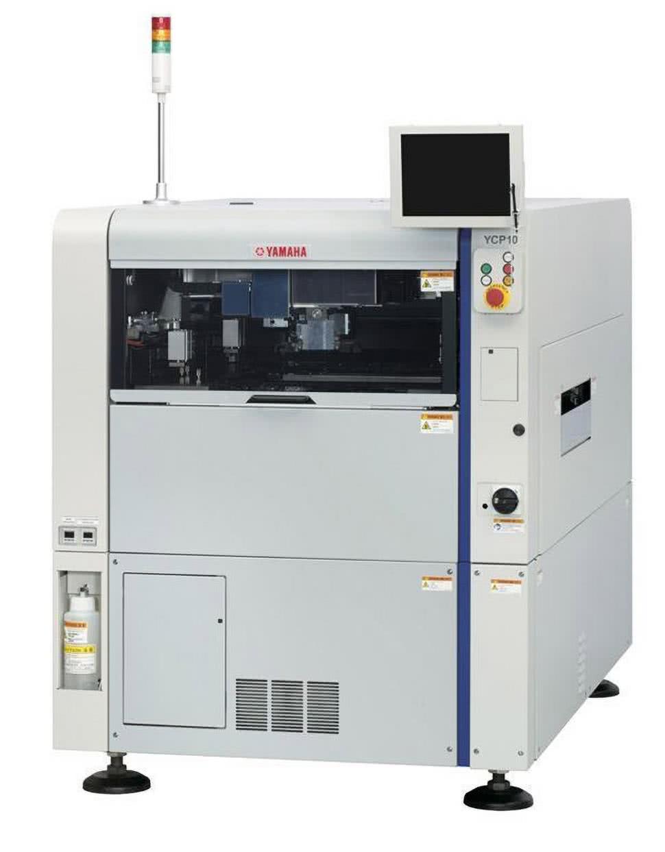
Many studies and researches on the efficiency of the soldering process emphasize the fact that about 70% of all soldering problems are generated by improper placement of solder paste in the solder printing process ( Photo 6). Using a professional YAMAHA YA-YCP10 solder paste printer ( Photo 7) will avoid such situations.


Soldering
Once the components are properly laid out on the surface of the board, the soldering stage proceeds. For circuits with predominantly surface mount components, reflow soldering is the most efficient type of soldering. In this technique, a PCB with components arranged on it passes through an oven divided into several zones, maintaining different temperature values in each of them. The temperatures in each zone are selected depending on the details of the circuit design in such a way as to ensure maximum efficient solder flow and the formation of high-quality solder joints but at the same time taking into account the thermal sensitivity of the components. An example of a temperature profile is shown in Figure 5.
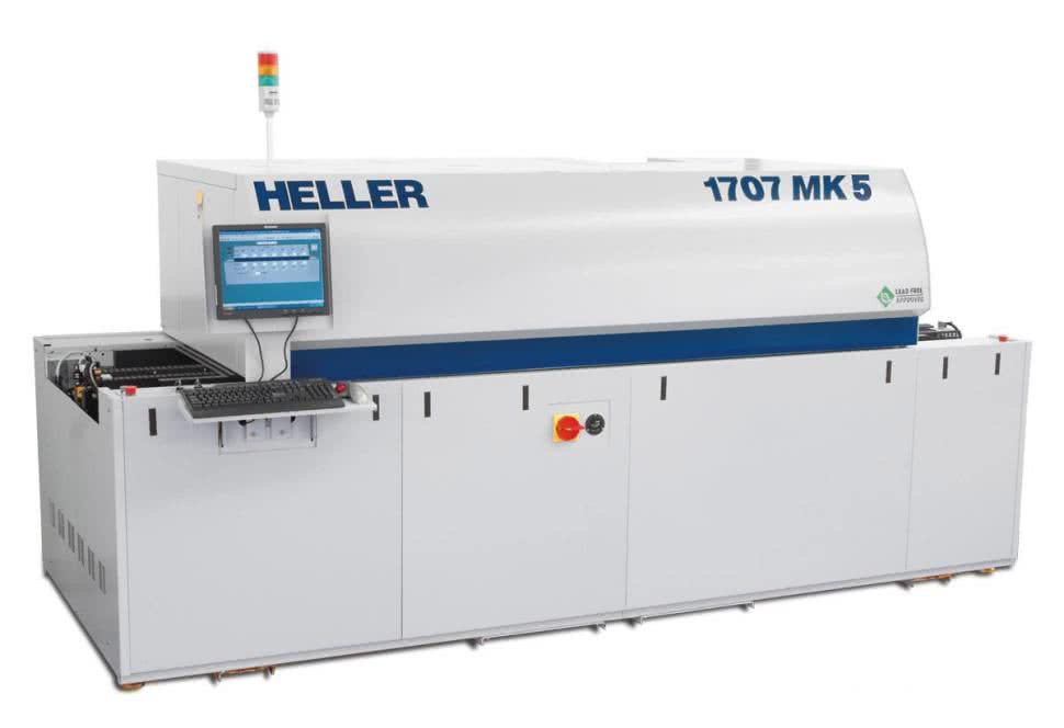
One of the top developments in reflow soldering is the flagship product of the world’s largest reflow oven manufacturer, HELLER Industries – HE-1707MK5 (Photo 9). It is a device equipped with 7 heating zones with upper and lower heaters with ±1°C temperature stabilization and one cooling zone allowing temperature extinction of >3°C/s. The precision of this order realizes even the most stringent requirements of lead-free profiles. The process can be carried out in a nitrogen environment, and the unit is equipped with a Uniform Gas Management System that eliminates nitrogen flow losses and reduces nitrogen consumption by up to 40%.


Conclusion
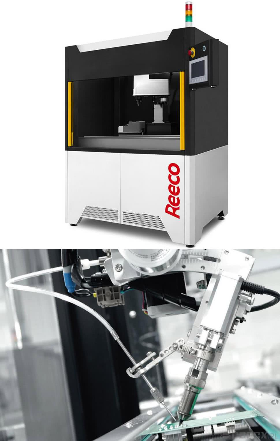
Complementing the production lines are solutions for automating THT assembly. Conventionally, soldering waves are used in this process. For small batch production, however, precision soldering robots, which do not require heating the entire crucible of solder and can be quickly reprogrammed from one batch realization to another, are more cost-effective. The best example of such a solution is the REECO soldering robot (Photo 10), which many fans of sports soldering have had the opportunity to see at various industry events in Poland and Europe competing against soldering champions for time.
The solutions discussed here can be seen and tested at the RENEX Technology Center. The right choice of equipment is the key to the success of any manufacturing activity. The mission of RENEX Group is to provide comprehensive equipment for the electronics industry and to support its development in Poland and Europe.
