Today’s AOI systems, which are most often found at the end of the production line, are capable of detecting almost all visible defects in assembled electronic packages. As technology advances, however, the pressure to improve these systems does not diminish.
New SMT component packages, including smaller SMD passive components and so-called chip-scale semiconductors, present difficult challenges requiring ever-increasing resolution. In addition, components with relatively large sizes are still being used. In the automotive sector in particular, components such as certain types of connectors conform to industry standards that are maintained from generation to generation. As a result, the range and variety of component sizes that inspection systems must handle is increasing.
Multilayer SMD production has also become more affordable in recent years than it was in previous decades. For this reason, their use – as a method of miniaturizing end products – is increasing. This is compounded by the fact that surface-mounted components are increasingly densely distributed, which further poses greater challenges in terms of lighting and cast shadows. In addition, as assembly complexity increases, each board contains more components that must be inspected.
Overcoming historical obstacles
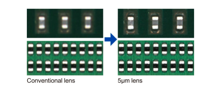
Maintaining image sharpness as the observed elements decrease depends on three aspects: optimal lighting, camera resolution and lens characteristics. In the latest YRi-V 3D AOI system, YAMAHA has used a 12Mp camera with an improved 5µm lens option (Figure 1), in addition to 12µm and 7µm lenses.
In the course of high-speed inspection, the high-resolution lens works in conjunction with the new YRi-V coaxial illumination system developed for finding tiny defects. This makes it possible to inspect even the smallest components such as 0201. The aforementioned coaxial illumination can be used in automatic inspection systems even at the level of a single inspection step, enabling YRi-V to identify defects such as scratches and cracks in components such as wafer-level chip-scale packages (WLCSPs), which have a shiny, reflective surface.

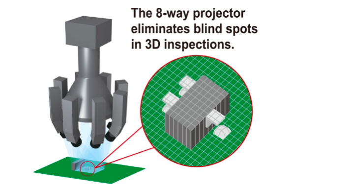
Along with increasing the lens resolution to 5 µm, the image processing subsystem has been improved, using the latest generation of graphics processing units (GPUs). This has made it possible to speed up the inspection cycle time by 60-100%. The combined effect of the improved lens and processing technology provides a simultaneous increase in resolution and inspection performance. Apart from increasingly smaller component sizes, the aforementioned multilayer packages are also a significant inspection challenge. This is especially true for small components, such as SMD chips, which can cause so-called blind spots when placed next to larger parts, preventing a clear view of the larger component’s I/O pins and their assigned solder pads. Conversely, larger parts can cast a shadow on smaller components, such as SMD chips, when placed between them, making it impossible to assess the solder pins and the identification and polarity markings applied to them.
YAMAHA’s newly developed solutions, including the 8-way projector (Figure 2), available with the YRi-V system, effectively address these issues. The projector prevents shadows by ensuring that all elements in the field of view are evenly illuminated, and the expanded measurement capabilities allow close-up inspection while handling a wide range of element sizes, from the smallest to the largest. It should also be added that the maximum measurement distance has also been increased to 25 mm.

AOI enhanced with AI
While the performance of next-generation GPUs has enabled faster image processing and defect detection, artificial intelligence (AI) is poised to bring new capabilities to AOI – as it has for many other aspects of industrial and consumer technology.
This enables automatic selection of the optimal component library. Artificial intelligence is also used to support 3D measurement of components to generate data for components not found in any existing library, as well as to analyze captured images and support pass/fail evaluation. This combines the repeatability of a machine with the flexibility of human visual inspection. This allows for fast, accurate and repeatable pass/fail evaluation.
Four-angle inspection and algorithms
Looking at how automated inspection technology has evolved, solder defects have always been the most difficult for AOI systems to analyze. Some of them – such as “head-in-pillow” defects, which occur when solder fails to wet the tip of a component – are notoriously difficult to detect using conventional equipment and methods. Solder bridges are another example of a difficult-to-identify situation.
YAMAHA’s 4-angle inspection cameras can provide a solution to these problems by capturing images at an angle, allowing the system to capture a comprehensive image of the component being inspected. The YRi-V system introduces 20Mpixel cameras at the same time, allowing the system to simultaneously capture these images in even better quality. Combined with the new cameras, the improved 4D inspection algorithms use more image information to increase detection of problems such as the aforementioned bridging and “head-in-pillow.”
Generating programs and software
Some AOI systems provide optimal performance when installed in-line with other equipment running on the same software platform. A more open approach – adopted by YAMAHA, allows users to take full advantage of the AOI system’s capabilities when working with any type of in-line hardware. In particular, rapid program generation is made possible by YSUP software, which is available on an open and license-free basis.
The full-featured YSUP software can convert inspection data directly from CAD/CAM or YGX, and also supports gerber data as standard. In addition, the YSUP function in the YRi-V offline programming software allows AOI programs to be created from ODB++ data without the need for a YGX file. If a silk screen PCB is present in the ODB++ data, it can be imported as a simplified image to facilitate positioning of new components using the offline programming station. This prevents developers from having to take over the factory AOI system to scan the PCB and create a template image, avoiding interruptions to normal production.
The software automatically generates and displays virtual images of the production PCB, so operation of the system requires no special skills. Additional automated features include detection of any parts with through-holes, with the ability to generate appropriate inspection data. New functions are also available to assist in data tuning, including automatic detection of inspection windows based on component shapes and pad positions. In addition, the software automatically determines lighting parameter settings to ensure optimal illumination, minimizing trial and error and reliance on user experience. Automatic position correction based on the amount of component misalignment is also available, helping to minimize operator involvement. Together, these features can reduce data alignment time by up to 50%.
Conclusions
Today’s leading electronics assembly companies need AOI systems to help them further improve productivity. Solutions are needed for standard challenges, such as defects that are difficult to identify. On the other hand, the latest AOI systems also need to deal with the challenges of cutting-edge technologies, such as dense multilayer boards.
The latest image processing technologies, as well as cutting-edge techniques such as machine learning, are now needed to improve defect detection and speed up programming and image analysis. The new generation of AOI systems now entering the market also offers superior multi-angle illumination, enhanced image resolution, and easy-to-use configuration and management software.
EXCLUSIVE DISTRIBUTOR OF YAMAHA SMT and YAMAHA Robotics – RENEX GROUP
RENEX Group is the exclusive distributor of YAMAHA SMT and YAMAHA Robotics in Poland and Central and Eastern European countries. YAMAHA equipment, as well as other products from the RENEX product range, can be seen and checked in operation under production line test conditions, including on the company’s own components and subassemblies, at the RENEX TECHNOLOGY CENTER and DEMOROOM. In addition to equipment, RENEX Group provides a comprehensive range of consulting and advisory services in the field of production process automation.
In addition, RENEX Group has developed, manufactures and supplies turnkey robotic solutions – REECO Robots. Each robot is a fully automated, self-contained unit that can be implemented into an operating or newly established production line. The solutions meet the requirements of electronic package manufacturing – and other broadly defined industries. Available models allow automation of soldering, dispensing, conformal coating, labeling and bolting processes. On individual orders, the Group also develops, manufactures and supplies solutions to automate other processes.
