For lead-free soldering, not only specialist equipment is required, but also suitable solders, fluxes and PCB cleaners after soldering. This is what this article is focused on.
First of all, it is worth recalling why it was decided to make such difficult and costly changes in the technology of electronic equipment production. The harmful effects of lead on humans and their environment have been known for many years. Nowadays, when all kinds of electronic devices surround us from all sides, the threat has become very serious and something had to be done about it. The Japanese were the first to develop lead-free soldering technologies, and Panasonic produced the first personal CD player with lead-free soldering.
The European Union issued in January 2003 the Directive „On the restriction of the use of certain hazardous substances in electrical and electronic equipment“. Among other things, it prohibits the use of lead. This directive is known as RoHS (Restriction of the Use of Certain Hazardous Substances). In Poland, it was introduced by the Regulation of the Minister of Economy and Labour and announced in the Journal of Laws No. 229, item 2310. The provisions of the Directive enter into force on 1 July 2006.
SPECIFICITY OF LEAD-FREE SOLDERING TECHNOLOGY
Lead-free solders differ from those used previously, the melting point is about 30ºC higher, the surface tension is higher, the wetting of soldered surfaces is worse. Due to the limits of the components, the temperature window in which soldering can take place is narrowed. Therefore, it becomes necessary to set the process parameters more precisely and, moreover, to precisely control the connections made. Various types of soldering binders are used during soldering, also known as solder. For manual soldering, binders in the form of wires with a diameter of about 1 mm are used. They usually have one or more veins filled with flux to facilitate soldering.


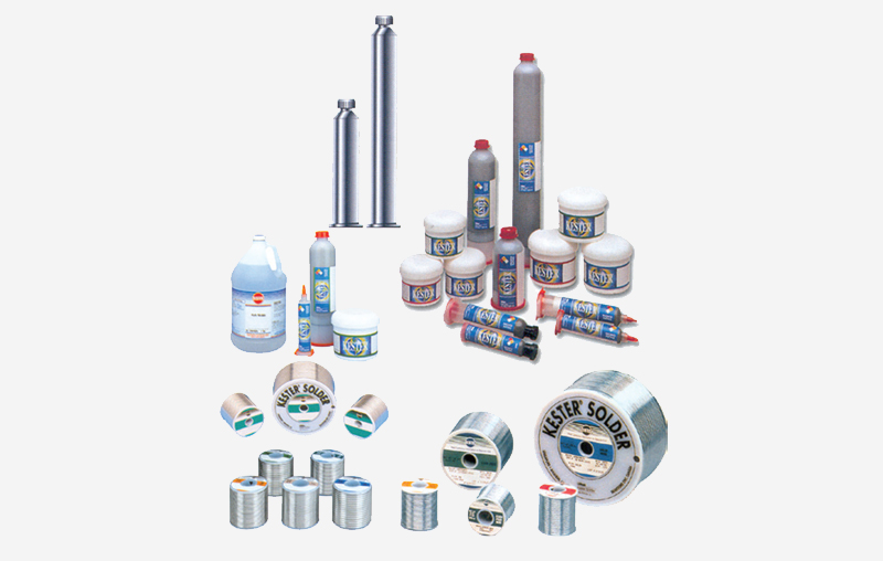
In industrial technologies, molten solder in bars or shot is used for wave soldering. For soldering surface mounted elements, soldering pastes containing grinded solder and flux are used. The basic component of all solder for lead-free soldering is tin, similar to solders containing lead. The difference is that lead-based solders contained about 65%, while lead-free ones have much more, at least 95%. The remaining components are silver and copper. Zinc, antimony, bismuth or indium are added less frequently. However, the content of each of them generally does not exceed 1%. Fluxes are also necessary for soldering. The fluxes do not help in melting the binder, e.g. by lowering the melting temperature. They make soldering easier by cleaning the surfaces to be joined. Two basic types are still used: colophony-based and synthetic fluxes. Among the latter, No Clean fluxes, which do not require cleaning after soldering, form a separate group.
Lead-free soldering processes vary depending on the purpose for which they are intended. It is obvious that soldering of single elements is done differently, e.g. when repairing electronic circuits, production soldering of THT elements that are mounted on boards looks different than soldering of SMD or BGA elements. Below are the basic technologies of lead-free soldering.
BRAZING
An essential condition for the correct connection of the elements is that the right amount of heat energy is supplied to the soldering point within a certain time. In order to meet this requirement, the temperature of the soldering tip should be about 40ºC higher than the melting point of the solder, therefore about 260ºC.
The soldering process, from the moment the soldering point’s tip touches the soldering point to the moment it is retracted, takes about 5 seconds. After touching the soldering iron, the binder reaches its melting point within a second. The flux is activated simultaneously. The binder melts on the soldered surface for approx. 4 seconds. When the soldering iron is removed, the binder solidifies and the soldered area cools down. For manual soldering there are solders in the form of wires, with the No Clean flux based on colophony, for example from Kester (e.g. with a diameter of 0.25 mm to 1.0 mm). The wires are made to an alloy of SN96.5Ag3.0Cu0.5 and have a melting point of 217ºC. Suitable flux for use in manual soldering are Kester fluxes based on colophony, e.g. in the form of gel in a syringe.
REFLOW SOLDERING
Different parameters of lead-free solder from those used so far – containing lead, set new requirements for soldering furnaces. First of all, it is necessary to pay attention to a significant reduction in the safety margin. This is about temperatures. More sensitive semiconductor components cannot be heated above 260ºC. In lead alloy soldering furnaces the temperature did not exceed 220ºC, so the safety margin was 40ºC. When soldering with lead-free alloys the temperature is about 250ºC. Therefore a much smaller margin of 10ºC remains.
Lead-free soldering furnaces must enable faster heating of the fill to higher temperatures and provide much greater accuracy in setting and maintaining temperature. An example of a soldering profile in a flow oven with a total cycle time of 5 minutes consists of several phases: heating 60 seconds from ambient temperature to 150ºC, heating 90 seconds to 180ºC, soldering 60 seconds – in this phase the temperature rises to about 240ºC, cooling 90 seconds, to ambient temperature. The illustration showing this profile shows the differences from soldering with alloys containing lead. It is noticeable that the soldering temperature is about 35ºC higher and the whole process takes longer.
In lead-free soldering, the cooling of the tiles is essential for the quality of the connections. Cooling too quickly reduces mechanical strength and also worsens the connection structure. Besides, the flux of the soldering paste may not evaporate in time. Lead-free soldering pastes must therefore be adapted to a profile with a higher soldering temperature and longer duration. A good soldering paste must have properties that ensure the reliability of the connections. It should have sufficiently fine particles (balls) of the binder, not differing in size, so that, when applied to a small surface, they do not distort its geometry. It must adhere well to the substrate and not move (run down) on it, and at the same time cover it thoroughly. The flux contained in the paste should evaporate completely after soldering, leaving no residue.
All these features are checked by the manufacturer for compliance with the relevant standards. Kester offers the following types of paste for reflow soldering. „R905” – No Clean paste, available with a solder of various alloys and modern flux, to be applied to the substrate by printing, fine-grained, not flowing off the surface. Can be used in normal atmosphere or with nitrogen. The second paste – R520A – has similar properties to the previous one, but can be used on substrates that are more difficult to solder. After soldering the boards should be washed with hot water.
WAVE SOLDERING
Soldering in wave technology with lead-free binders creates more problems than reflow soldering or hand soldering. Wave soldering units not only have to meet the requirements previously mentioned when discussing ovens. There are also requirements for crucibles with molten solder. Lead-free solder has a stronger chemical effect on the steel of which the crucible is made. Therefore the soldering crucible is made of special alloy steel or must have a covering, e.g. of ceramic material. Unfortunately, older soldering waves cannot be adapted to lead-free materials – even if technologically possible, the costs of modernization render such investment pointless.
When switching to lead-free technology it is necessary to select a new binder with the appropriate composition and a new type of flux. Suitable for wave soldering are alloys with silver content, e.g. Sn96,5Ag3,0Cu0,5, or two-component alloys, e.g. Sn99,3Cu0,7. Binders containing silver are naturally more expensive, but the disadvantage of two-component binders is higher melting point. For these applications, Kester offers a two-component binder with a melting point of 227ºC, available in bars. It is equally important to select the right fluxes as they need to be more active and act a little longer to ensure both good covering of the parts to be bonded and a good joint structure, without holes or cracks. Liquid, No Clean and water soluble fluxes are used for lead-free wave soldering.
Kester offers both No Clean and water soluble fluxes. In addition to the above information, it is worth adding that also the conductive paths and ends of the assembled elements must have coatings adapted to lead-free technology.
REPAIRS OF SYSTEMS WITH BGA AND CSP COMPONENTS
In discussing the principles of manual soldering earlier, attention was drawn to both the difficulties associated with higher soldering temperatures and higher surface tensions, as well as the more difficult joining of elements in the case of lead-free binders. Even greater problems arise during repairs – replacement of BGA and CSP elements.
The temperature/time profile is more complex than in lead soldering and runs at higher temperatures. Both the solders and fluxes used in repairs do not differ in chemical composition from those used in other lead-free soldering processes.
It should be reminded that semiconductor components have a limit temperature of about 260ºC and the heating medium will have a temperature of about 245-250ºC. The margin is only 10-15ºC. When repairing, you have to forget about the soldering iron at all, especially since there are usually several hundred soldering points to be soldered at the same time, and they are completely hidden.
CONTROL OF SYSTEMS AFTER SOLDERING
The RoHS Directive concerns not only lead but also several other metals: cadmium, hexavalent chromium, mercury and certain organic compounds. It is therefore necessary to control the materials and components used by electronics manufacturers to check that these products do not contain prohibited materials. Modern technology has a variety of analysis equipment. These include e.g. mass spectrometers, gas chromatographs, electron microscopes, X-ray equipment.
All these tests need not be carried out by electronic device manufacturers if they have reliable component suppliers. On the other hand, electronics manufacturers need to check the quality of their products very carefully after the introduction of lead-free technologies, as these technologies are more difficult to mass produce and soldering defects may occur more often. There are many different connection defects. So many that it is impossible to mention them all here. A few examples are enough. In the case of THT assembly, for example, you will find that the metallized through-hole is not completely filled, or that the conductive path is inaccurately covered with a solder. In CSP/BGA systems it happens that not all contacts are soldered or a short circuit between adjacent ends is formed. Regardless of the technology used, it is necessary to check the boards after soldering. It is relatively simple in the case of THT mounting or SMT, because you can see both conductive paths as well as components and soldering points.
In these cases, optical devices are used, ranging from ordinary magnifying glass to a stereoscopic microscope. Problems begin when you need to check the correctness of CSP/BGA chip connections, because the soldering points cannot be seen. This is when X-ray equipment comes in handy. There are many models of devices for checking the boards. For an overview, here are some solutions.
A wide range of high-end optical inspection equipment is available from Vision Engineering Ltd. The model called Mantis combines the advantages of a monitor and microscope. Further advantages are light control and high resolution of the viewed image. Interchangeable lenses provide magnification from 2x to 10x. The Mantis UV variety allows to control using ultraviolet radiation. The most technically advanced devices, e.g. Hawk, allow not only inspection, but also measurements in X, Y, Z axes, with an accuracy of 2 microns.
The measurements are made and processed by means of a microprocessor. The XR-3000 or XR-4000 device of a well-known American company PACE is used for measurements and control with X-rays. The camera of the device with a zoom from x7 to x40 allows to detect defects with an accuracy of 25 microns. The device can cooperate with a video monitor and BGA mounting devices.
CLEANING THE BOARDS AFTER SOLDERING
Once the board has been assembled, it is usually necessary to remove the contamination from the board. Contaminants are remnants of the soldering paste or the flux itself, e.g. in the case of wave soldering. Lead-free technology requires higher temperatures and more active fluxes. Therefore, greater difficulties in removing impurities could be expected. However, it turned out that there are no major problems with this. Micro Care has the right products in its production programme for all applications.
For example, for the removal of colophony-based flux residues, there is a product called SuperClean, which is strong but non-flammable and non-toxic. No Clean type of flux residues removes VeriClean, safe for plastics, quick-drying, environmentally friendly. For the removal of residues of water-soluble fluxes, on the other hand, there is an agent called Flux Remover C, which has a similar effect to the previous one and also removes No Clean flux residues.
CONCLUSIONS
Lead-free technology is undoubtedly much more difficult to use because it requires higher temperatures, and the tolerances for the duration of individual operations are also narrower. Moreover, more chemically active products are used. Dangers for boards and components are mainly related to high temperatures and chemical exposure. Therefore, production equipment and consumables must be of high quality, which only reputable companies can provide. Once these conditions are met, the expected quality and production efficiency will be achieved.