Standards in the electronics industry are the foundation of a successful business. Finding a common language between the contracting authority and the contractor is extremely important. By setting standards known to both parties, we avoid misunderstandings, accelerate the process and ensure quality.
Standards for electronics industry were created and developed by a non-profit US association – IPC – Association Connecting Electronics Industries, founded in 1957 under the name Institute for Printed Circuits. The standards related to the production of electronics developed by IPC are constantly created, updated, expanded and detailed.
These processes are carried out thanks to industry specialists who actually use these standards in their daily work. The consequence of this approach is not surprising – today the standards created by IPC are used by the whole world. Regardless of whether we work with a subcontractor from the Far East or with contracting parties from Western Europe, the language of IPC electronic standards is easily understood by everyone. Getting to know the rules of conduct requires first of all finding a good teacher.
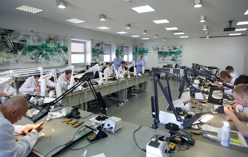
In Poland, training in IPC standards is offered by the IPC Authorized Training Center run by RENEX from Włocławek. The offer includes theoretical and practical courses from all IPC standards – from the quality standards to the assembly of electronic circuits (the so-called 610) to the requirements for the installation of cables and wire harnesses (the so-called 620).
Behind the Authorized IPC Training Center is 20 years of experience, thousands of trained people working in hundreds of companies in dozens of countries on several continents.
Some of the lecturers have been associated with the IPC Authorized Training Center from the very beginning, which supports their experience and allows them to conduct courses and grant authorizations even at the level of an IPC Certified Trainer.


COURSES FOR PCB DESIGNERS
Due to the theme of this issue, we’ll look at courses for PCB designers.
Both independent design offices and manufacturers with internal laboratories and design departments use them.
For them it is particularly important that the circuits they produce are fully compatible with the specificity and capabilities of the production line.
Implementation of projects that are objectively wrong or do not match the specific production line may result in an increased percentage of incorrectly assembled PCBss, which in extreme cases may affect the profitability of a given device.
A common problem is a bad adjustment of the dimensions of the THT elements to the technology in which the manufacturer operates. Failure to take into account restrictions resulting, e.g., from the use of a solder wave, may lead to violation of the electrical distance rules, and even the need for manual corrections of the entire lot.
An example of an objective design error, regardless of the manufacturer’s standards, is also the incorrect distribution of mass fields. Their uneven positioning may cause the plate to warp in the reflow oven during heating (deformation) and, as a consequence, insufficient adhesion of the BGA components.
This type of situation is dangerous because it can result in a hidden defect that will only become apparent after a few months of use.
Such a problem appeared about 10 years ago in the first Xbox consoles, which forced the manufacturer to replace the warranty covered equipment on a large scale and to perform many post-warranty repairs. For the electronics market, this error meant an increase in sales of service equipment, but at the same time was a big blow to the manufacturer’s brand. As you can see from this example, erroneous projects, including projects ill-suited to the production technology of a given manufacturer, can result in painful losses. For smaller companies this can lead to bankruptcy.
With such high stakes, communication between the PCB designer and manufacturer, the highest possible industry standards and the use of expertise to create the project are crucial.
WHAT COURSES?
IPC education standards for printed circuits are defined at two levels: Certified Interconnect Designer (CID) and IPC PCB Advanced Designer Certification (CID +).
RENEX Authorized IPC Training Center – provides both of these courses. The CID course is suggested for PCB designers with at least 2 years of practical experience. It allows you to learn about IPC standards and how to implement them in practice in your projects. This applies in particular to such issues as alignment and routing techniques, thermal management, physical characteristics of the PCBs, assembly of components or surface treatment of the plate.
Knowledge of these issues provides the basis for proper decision-making processes in the company in the field of creating PCB designs that will be universally understood and in line with international standards.


Only specialists with a CID level certificate can take the CID + course. The training significantly extends knowledge of IPC standards and allows you to verify it. The course thoroughly analyzes issues such as material properties, electrical parameters, including proper component placement techniques, power supply and grounding processes, and dimensioning and documentation.
Completing the course enables proficient use of IPC standards and equivalent project activity in global markets. When thinking about convenience, it is worth mentioning that a fully equipped hotel and restaurant base is available for course participants organized by RENEX.