In this article, we look at the range of applications for one of the key devices used
in the electronics industry – the digital microscope.
Market pressure forces manufacturers to further miniaturize electronics. New phones, computers or other multifunctional devices coming out every year have to be more and more efficient without increasing their size in order to be competitive. As a result, electronic packages use smaller and smaller components in ever greater density. This causes a domino effect forcing not only the manufacturers but also their subcontractors and service providers to adapt to the realities of working with highly miniaturized electronics.
This problem can be seen well at the optical inspection stage. The bench magnifiers with illumination that have been used so far are now largely becoming a preliminary tool that is only useful for a cursory inspection of the entire electronic package. The magnifications of 1.7x to 3x that they achieve are far from sufficient when working with the smallest electronic components.
Microscopes have become a common answer to this problem. Here it is important to distinguish between the two most common types of these devices: stereo microscopes and digital microscopes.
Stereo microscopes are well known devices and used in almost all branches of science and industry. Based on pure optics, they are almost ideal inspection devices. By extending the capabilities of the human eye, they allow for very accurate, spatial vision of the points being approximated. However, this design has seemingly minor drawbacks, making their digital counterparts much more popular today.
The first disadvantage is that it forces one body position on the operator. The user of the device must bring his eyes close to his glasses and remain in this position until the work is finished. In the case of, for example, supplementary assembly in a production line, this may involve working for days in a position that is bad for the back. The obvious consequence is an increased risk of occupational skeletal disorders and eye or headaches. The second disadvantage is that simultaneous work on the device is limited to one person.
All this makes the digital microscopes, also called video microscopes, increasingly popular in the electronics industry. In its simplest form, these devices are based on a digital camera with a lens adapted to macro photography with a high zoom, transmitting the image live to a monitor.
Unlike the previously discussed conventional stereo microscopes, the operator has the ability to position the monitor and view the image at a location of his or her choosing, and to work in a non-descending position. The image can also be analyzed by several complementary specialists at the same time, and, given the ability to transmit the image remotely, also by specialists and consultants working remotely. The opportunity for dialogue and collaboration brings new, more dynamic ways of working, greater inspection confidence, security, and innovative ideas.
Devices of this type allow you to obtain a zoom greater than the stereo microscopes – up to 600x and usually work in Full HD resolution. The only limitations of these devices are those arising from the principles of photography itself. The tonal range of digital camera sensors is not as large as that of the human eye – which means that at high magnifications very dark areas and very bright ones may be underexposed or overexposed. In most cases, however, these factors are not a problem, and digital microscopes are today’s most popular inspection solutions for widespread use.
All this makes that in the electronics industry, digital microscopes are most often used in production lines for complementary assembly and in repair and modification stations. A wide range of digital microscopes of TAGARNO brand, which is very popular in Poland, deserves a special attention.
In business for more than 50 years, Danish company TAGARNO is one of the world’s leading manufacturers providing inspection equipment used in fields such as materials science, automotive, agriculture, food production and the electronics industry. Renowned for the quality of its products, the company specializes in producing top-of-the-line digital microscopes and developing software to develop their functions.
The first to fit the needs of the electronics manufacturing industry is the TAGARNO TREND FHD model. These microscopes display on the monitor a real image with the highest color reproduction and sharpness transmitted by the camera in Full HD resolution without interference and delay. In addition, the available working space – between the observed object and the camera lens is up to 333 mm which allows not only the inspection but also comfortable work with most of the tools used in the electronics industry. All this makes the devices ideal for work at repair and modification stations.
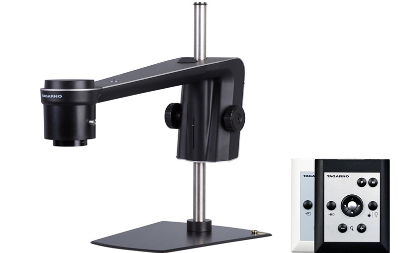
Digital microscopes are also used in line trains for in-process inspection. In this application, the main task of the microscope is to enable the operator to carry out quality control and process control at individual stages of the production process. Devices in a similar range are also used in design departments – when building prototypes. Here their particular role – apart from the possibility of inspection – is the possibility of archiving the progress of conducted works and potential imperfections in the process and created electronic package. The TAGARNO ZAP FHD is a device optimally fitting into this range of tasks. This device has a controller built into the camera which eliminates unnecessary cables and is mounted on a multi-axis stable arm. All this ensures great comfort of use and easy positioning of the camera lens over the controlled PCB.
To facilitate the operator’s ongoing quality and process control, TAGARNO also supplies a wide range of software for use in the electronics industry. The first example is the Image Comparison App – which allows the efficient comparison of two images. This is particularly important when inspecting a manufactured wafer against a reference wafer.
The software allows two images to be superimposed, viewed side-by-side, alternated, and zoomed and panned simultaneously, allowing the operator to efficiently navigate through the pattern image and the electronic package being inspected.
Using the second available program – Measurement App – the user can very precisely measure distances and angles between his selected points on the surface of the analyzed object. The tool also enables automatic calculation of surfaces – including irregularly shaped fields and holes. Apart from the application in the inspection of the electronic packages themselves, the software also proves useful in checking the compliance of the screen with the design submitted for execution. This is especially important in cases where there is a reasonable suspicion that the holes in the screen have not been properly sized relative to the pads on the plate. Failure to detect such an error at an early stage of production may lead to the pads falling into the hole in the sieve and, as a consequence, to covering too much pad area with a thinner than proper layer of solder paste. This in turn can result in a tombstone effect or even short circuits when the pad is dense.
The third popular software is Verification Lines App. It allows you to add a grid of reference lines to a downloaded image, specifying optimal values and their tolerances. The tool is particularly important in the assembly and inspection of components that are aligned with the outer casing of the device, such as various types of sensors. If the component is not precisely aligned with the device, it is possible that the housing will not close, stresses will occur that weaken the component’s attachment, or the fit will leak.
An extension of the possibilities arising from the three previously discussed types of software is the DXF Overlay App – streamlining the process of finding a component or component type on a board. This tool is particularly useful in the prototyping process, e.g. when a component needs to be changed for another one (of higher or lower value). By overlaying a DXF file on the PCB image being processed, the software enables finding the exact position of components with the help of the search engine. It significantly improves the process especially in case of complex electronic packages that may consist of hundreds of components.
All types of software discussed above also provide the possibility of adding notes to the analyzed images. This, together with the ability to easily save images at different stages of the production or prototyping process, makes it possible to document the progress of work, detected errors and introduced technological solutions.
SUMMARY
Digital microscopes, together with progressive miniaturization of manufactured and serviced electronic packages, are becoming an indispensable tool in service and production companies. Choosing the right solution should be preceded by consultation with an experienced consulting partner and testing of the device in operation within your own business.
The RENEX Group, one of the largest and longest operating Polish companies in the electronics industry, is a distributor of TAGARNO hardware and software in Poland. Within the framework of its mission to support development of the electronics production and service industry in Poland and Central-Eastern Europe, it provides interested entrepreneurs with far-reaching consulting, training and service support.
Equipment from the RENEX offer can be tested in operation in the RENEX TECHNOLOGY AND TRAINING CENTER and in the RENEX DEMOROOM in production line test conditions, also on your own components and subassemblies. RENEX specialists provide comprehensive assistance in the selection of appropriate equipment and conduct training on its correct operation – so that the user can fully exploit the possibilities of the equipment and software. The Group also provides technical support services including warranty and post-warranty service.
RENEX Technical and Sales Consultants, who have demonstration devices at their disposal, conduct free-of-charge product presentations at customers’ premises in order to select the optimum solution for a given problem. Customers therefore do not have to worry that the product they purchase will not meet their expectations.
If you are interested, please contact RENEX Technical and Sales Consultants – dth@renex.pl.