Electronic circuits are gradually miniaturized. Increasingly smaller dimensions and increased packaging of elements in the semiconductor structure makes the circuits more sensitive to electrostatic discharge. Protecting them from the effects of such discharges brings measurable benefits resulting in lower production costs (less faulty components), improved product quality and increased satisfaction of potential customers.
As the dimensions of electronic circuits decrease, their sensitivity to ESD electrostatic discharges or surges increases. Increasing requirements for ESD protection of components cause increased production costs. As a result, some companies producing electronic components have reported the need to lower the high ESD security requirements. Reducing ESD requirements for components will force manufacturers of electronic systems to invest more in protecting their own production lines.
WHAT IS AN ESD?
ESD (Electro-Static Discharge) is the flow of charges between objects with different electrical potential. Electrostatic charges arise when two different materials are rubbed together or when they are similar. The following contribute to the formation of electrical charges: walking on a synthetic floor, rubbing synthetic parts of clothing, moving plastic containers, unwinding adhesive tape, etc. The resulting electrostatic voltage has a high value.
ESD (Electro-Static Discharge) is the flow of charges between objects with different electrical potential. Electrostatic charges arise when two different materials are rubbed together or when they are similar. The following contribute to the formation of electrical charges: walking on a synthetic floor, rubbing synthetic parts of clothing, moving plastic containers, unwinding adhesive tape, etc.
The resulting electrostatic voltage has a high value. In a typical working environment it exceeds 10 kV, but at low humidity (below 20%) it can be as high as 30 kV. Approximation of two objects with different potentials causes the charge to jump from negative to positive potential (Fig. 1).


The damage caused by undesirable „jumping“ of electrostatic charges can be divided into two types: The first is so-called hard damage. This is damage whose effects are revealed immediately. The device is unfit for further use (this is permanent damage) and does not pass quality tests. The second one is soft damage. The device most often passes quality tests at the factory and is suitable for further use, but its performance is worse than typical. The effects of soft damage may become apparent during the operation of the device by the customer. The device may be faulty or even permanently damaged in a short time.
It is therefore an important problem to properly protect both the electronic system itself and the workplace where components and ESD-sensitive systems are used and produced. Damage can occur at any of the following stages: production, testing, storage, packaging, transport and use.
ESD MATERIALS AND PROTECTIONS
For ESD protection, shielding, conductive, charge dissipating and insulating materials are used. These materials are classified according to their surface resistance. The ESD shielding materials include materials with a surface resistance (the so-called resistance per square – resistance of a square cut of material) less than 1 kV.
An example of an ESD discharge shield is the Faraday cage, which suppresses and weakens the energy of the electric field. The most common shielding materials are metals and carbon. The task of conductive materials (surface resistance less than 100 kV) is to quickly move the charge through the material to be earthed.
Load-dispersive materials are defined as those with a surface resistance of 105…1012V. Charges flow more slowly to the ground than conductive materials, but this reduces the dangerous high electrical potential. Isolating materials are materials with a surface resistance greater than 1012V. Since such materials are difficult to ground, electrostatic charges remain on their surface for a long time. Examples of insulating materials are: glass, air, commonly used plastic packaging.
PERSONNEL SECURITY
In order to protect against high-value electrostatic charges it is necessary to use suitable conductive and dissipative materials. It is also important to use an earthing system that equalizes the electrical potential of components and personnel. A safe workplace is one in which earthing connects the workplace to the ground to equalize their potential. It is also very important to train personnel to follow the recommendations for electrostatic protection.
The most important element of earthing a person working with components is an esd antistatic wriststrap. It is an effective way to remove charges from the body. The wriststrap is connected by a copper wire to the earth or earth bonding point (EBP). In many cases it is necessary to use special antistatic footwear or an antistatic shoe strap. For ESD protection to be correct, footwear should come into contact with an ESD mat or earthed and conductive floor. Floors made of insulating material maintain a charge on their surface, which can cause electrostatic discharge. A special antistatic workwear is an ESD enhancement. The conductive fibres sewn into the material form a Faraday cage, which provides protection by suppressing static electric fields.
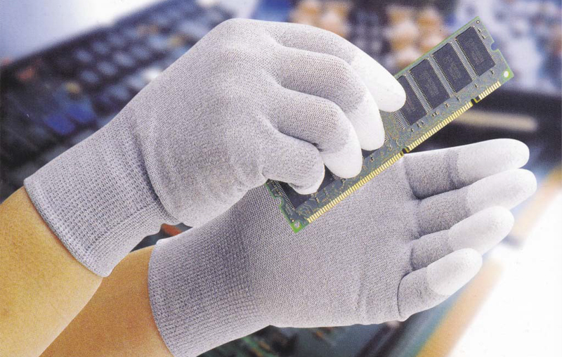
All parts of the clothing should have an electrical connection, which ensures proper discharge of charges. ESD gloves shall complement the ESD protection, especially for particularly sensitive parts. An unprotected hand does not ensure that charges are drained quickly enough.
AIR HUMIDITY
One of the most important environmental factors in ESD protection is relative humidity (Rh). Low air humidity (below 30%) favours the accumulation of electric charges on the surface of insulators (so it is important to measure ambient temperature and relative humidity). In such cases, ionizers are used. They are also used when earthing is not possible, through a system of appropriate cabling, or when this cabling prevents or significantly impedes operation.
Air ionizers work by spreading positive and negative ions. The ions come into contact with surfaces with positive and negative charges, so that dangerous charges are neutralized. Ion protection can be divided into local and complete.
In the local protection, station and air-gun ionizers are used (photo 6). Complete control consists in controlling the environmental conditions of the entire room. The amount of ozone produced by the ionizer should be taken into account. The maximum permissible level of produced ozone cannot exceed: 0.2 mg/m3.
EPA ZONE
An EPA (ESD Protected Area) is a space where there are no objects or activities causing damage to ESD-sensitive equipment. All dangerous discharges and charges are carried outside the EPA zone. In the EPA area the maximum allowable electric field strength is 100 V/cm. It is important to prepare a safe workplace (photo 7). All unnecessary objects, in particular food, bags, drinks, should be removed from it.
Before entering the EPA zone, each person should check personal earthing equipment with a tester. ESD protection elements should be checked periodically. A wriststrap should be checked daily as this is one of the key elements of electrostatic protection for personnel. The inspection of the cabling and the correctness of the connection of the mats to the ground must be carried out systematically (once a week). The surface of ESD mats should also be kept clean using specialised means. Commonly used cleaning agents leave an invisible insulating layer on the mat surface and may cause the accumulation of electric charges. Recommendations for ESD protection systems are contained in IEC 61340-5-1. Other ESD protection standards are listed in Table 2.
BEZPIECZEŃSTWO PODZESPOŁÓW I URZĄDZEŃ
Devices sensitive to electrostatic discharge should be stored with special care. For transporting components, conductive foams are most often used, which prevent potential differences of more than a few volts between the outputs (photo 8). In case of assembled PCBs, dissipative or conductive cuvettes, trays or holders for their storage are used (photo 9). Individual electronic packets are stored in appropriate bags, which should keep the charge level low, i.e. they should be made of dissipative or conductive material.